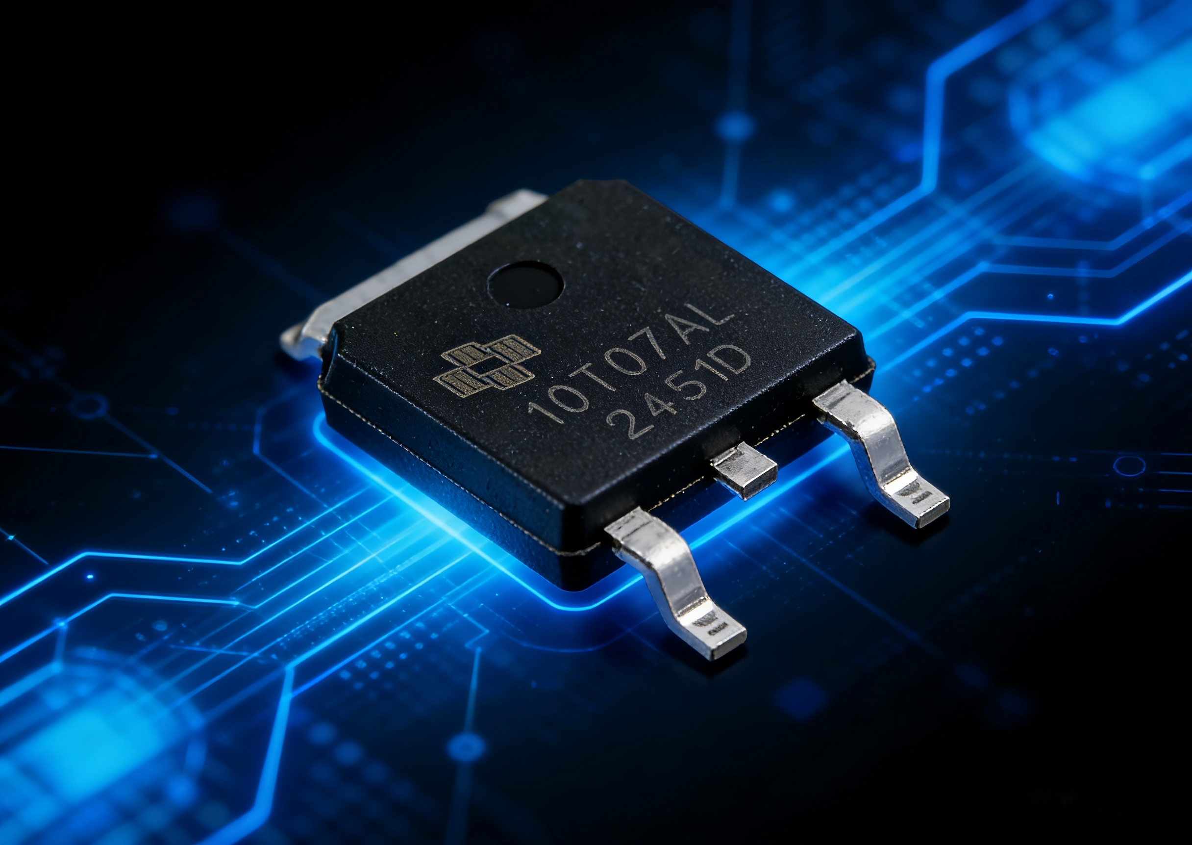
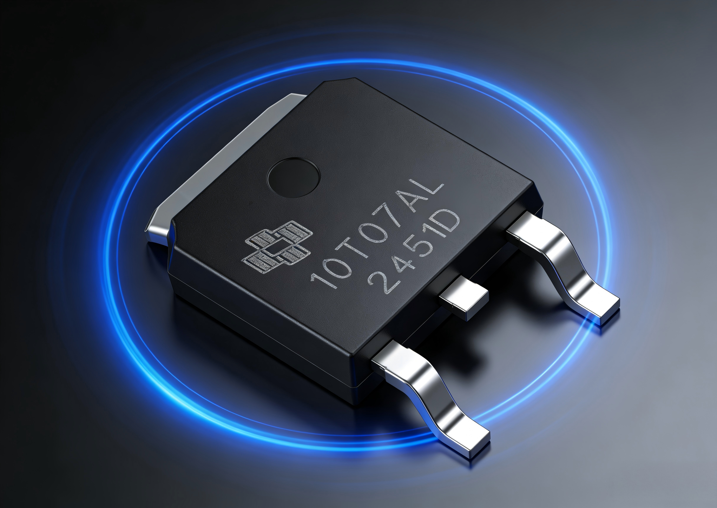
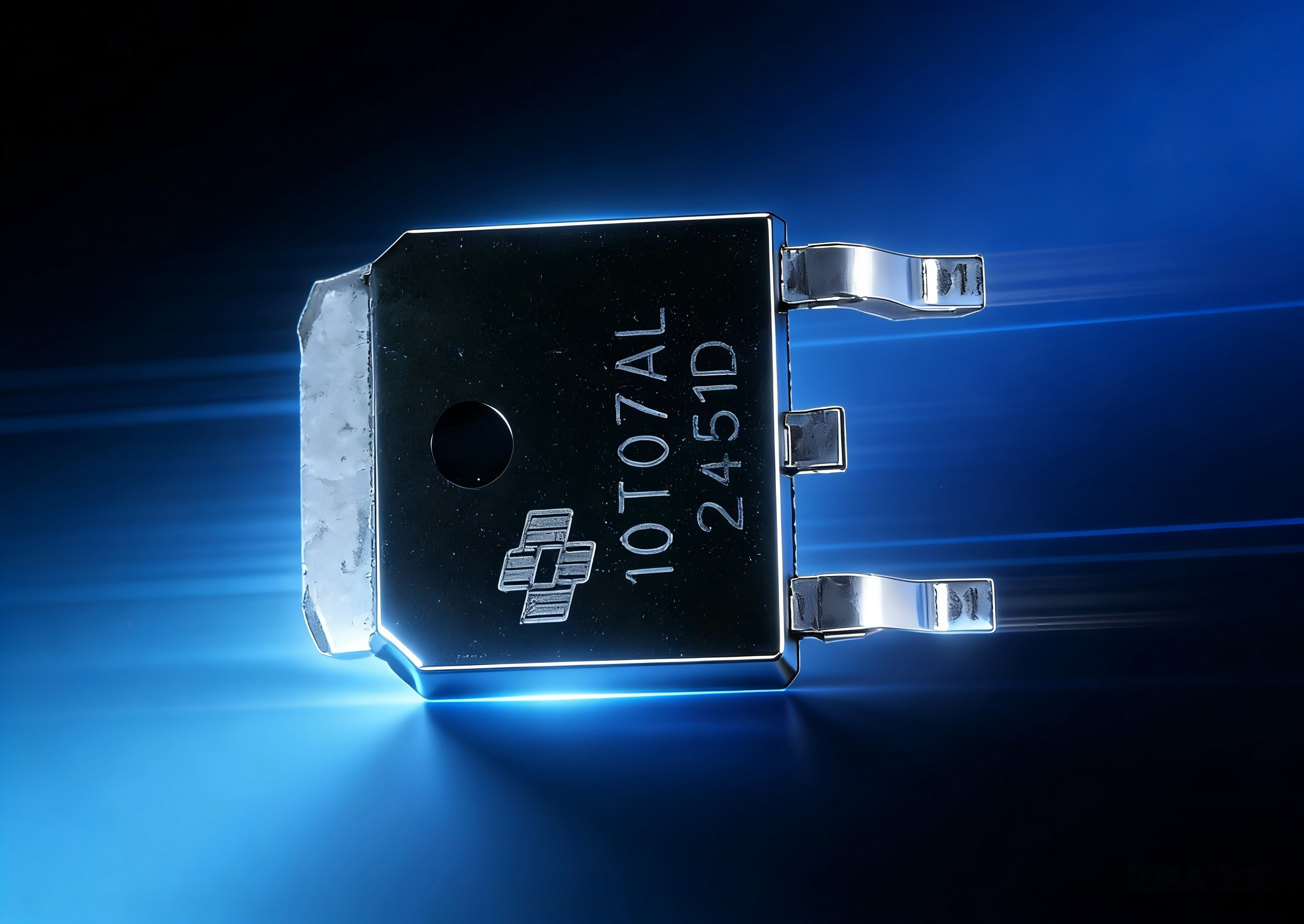


| Product Introduction of SMT10T07ALU 100V N-Channel Power MOSFET The SMT10T07ALU is a high-performance 100V N-channel power MOSFET packaged in the TO252-3L format. Boasting low on-resistance, an excellent figure of merit (FoM) and stable electrical performance, it serves as an ideal choice for high-frequency switching and power control in industrial, telecommunications and other fields. In addition, this product complies with halogen-free environmental standards, meeting the green design requirements of modern electronic equipment. |
Core Performance AdvantagesUltra-low on-resistance & excellent energy efficiencyAt VGS=10V, ID=20A, the typical static drain-source on-resistance RDS(on) is only 6.1mΩ, with a maximum value of 7.4mΩ. Even at low gate voltage VGS=4.5V and ID=15A, the typical RDS(on) is just 7.9mΩ, greatly reducing conduction loss and improving circuit energy efficiency. High current carrying capabilityAt a case temperature of 25℃, continuous drain current reaches 73A, and maintains a rated 46A at 100℃. Pulsed drain current is as high as 292A, making it suitable for high-current power control and heavy-load applications. Excellent figure of merit & reliabilityIt features outstanding FoM and is 100% tested for ΔVDS, unclamped inductive switching (UIS), and gate resistance (Rg). With single-pulse avalanche energy of 250mJ and single-pulse avalanche current of 31A, it delivers strong surge immunity and stable operation. Outstanding high-frequency switching performanceExcellent gate charge characteristics: total gate charge Qg is only 27nC at VGS=10V and 13.2nC at VGS=4.5V. Short switching delays: turn-on delay 4.6ns, turn-off delay 23ns, rise time 10ns, fall time 21ns. Combined with low input/output capacitance, it is ideal for high-frequency switching applications. Wide operating temperature rangeJunction and storage temperature range: −55℃ to +150℃. Ensures stable operation in extreme high/low temperature environments, adapting to harsh conditions in industrial equipment and outdoor communication devices. Key Electrical & Thermal ParametersMaximum Ratings (Tc=25℃ unless otherwise specified)
Core Thermal Characteristics
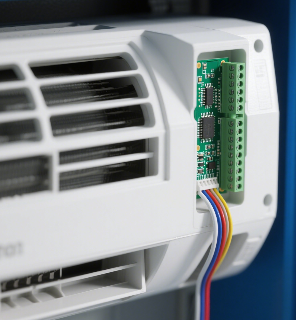
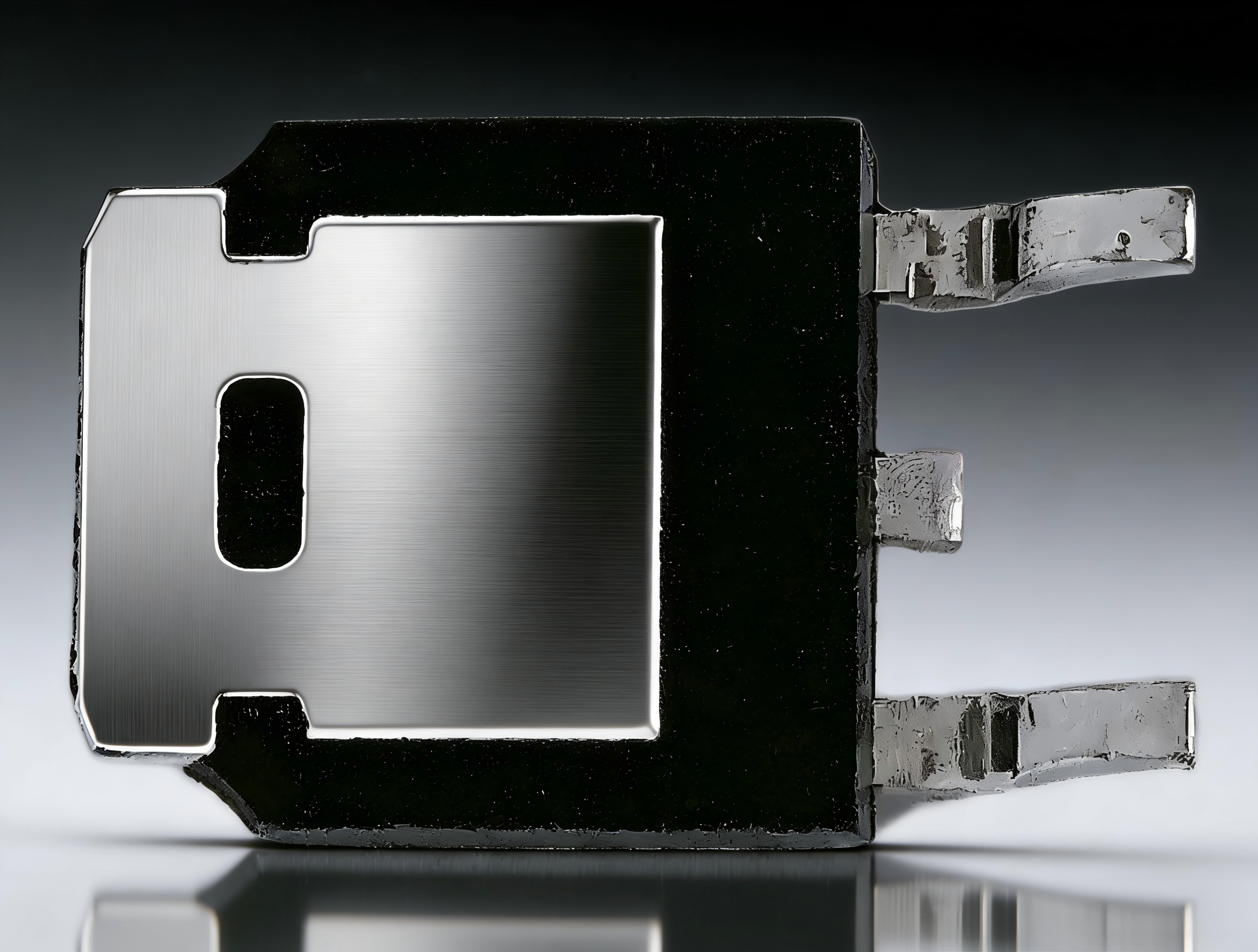
Excellent thermal conductivity effectively reduces device temperature rise and ensures long-term operational reliability. | Package and Mechanical CharacteristicsThe device is packaged in TO252-3L SMD package. The pin configuration (top view) is: D (Drain), G (Gate), S (Source). The package uses green molding compound, complies with UL 94 V-0 flammability rating, and has a moisture sensitivity level of Level 3 per J-STD-020.The package dimensions are standardized and compatible with standard SMT soldering processes. Optimized recommended solder pad design improves soldering reliability and thermal dissipation.It is supplied in 13-inch tape-and-reel packaging, with 2500 pcs per reel, suitable for mass production. Typical ApplicationsWith excellent electrical performance, the SMT10T07ALU is widely used in various power electronic circuits. Key applications include:
|
Ultra-low on-resistance and excellent energy efficiency: At VGS=10V and ID=20A, the typical static drain‑source on‑resistance RDS(on) is only 6.1mΩ, with a maximum value of 7.4mΩ. Even under low gate‑drive conditions of VGS=4.5V and ID=15A, the typical RDS(on) is just 7.9mΩ, significantly reducing conduction losses and improving circuit energy efficiency.
High current carrying capability: At a case temperature of 25℃, the continuous drain current reaches 73A and remains at a rated 46A at 100℃. The pulsed drain current is as high as 292A, enabling the device to adapt to high‑current power control scenarios and meet heavy‑load operating requirements.
Excellent figure of merit and reliability: The device features an outstanding FoM and is 100% tested for ΔVDS, unclamped inductive switching (UIS), and gate resistance (Rg). It provides single‑pulse avalanche energy of 250mJ and single‑pulse avalanche current of 31A, delivering strong surge immunity and stable operation.
Outstanding high‑frequency switching performance: With excellent gate charge characteristics, total gate charge Qg is only 27nC at VGS=10V and 13.2nC at VGS=4.5V. It exhibits short switching delays: turn‑on delay 4.6ns, turn‑off delay 23ns, rise time 10ns, fall time 21ns. Combined with low input and output capacitance, it is ideally suited for high‑frequency switching applications.
Wide operating temperature range: Junction and storage temperature ranges from −55℃ to +150℃, ensuring stable operation in extreme high and low temperature environments and adapting to harsh working conditions such as industrial equipment and outdoor communication devices.