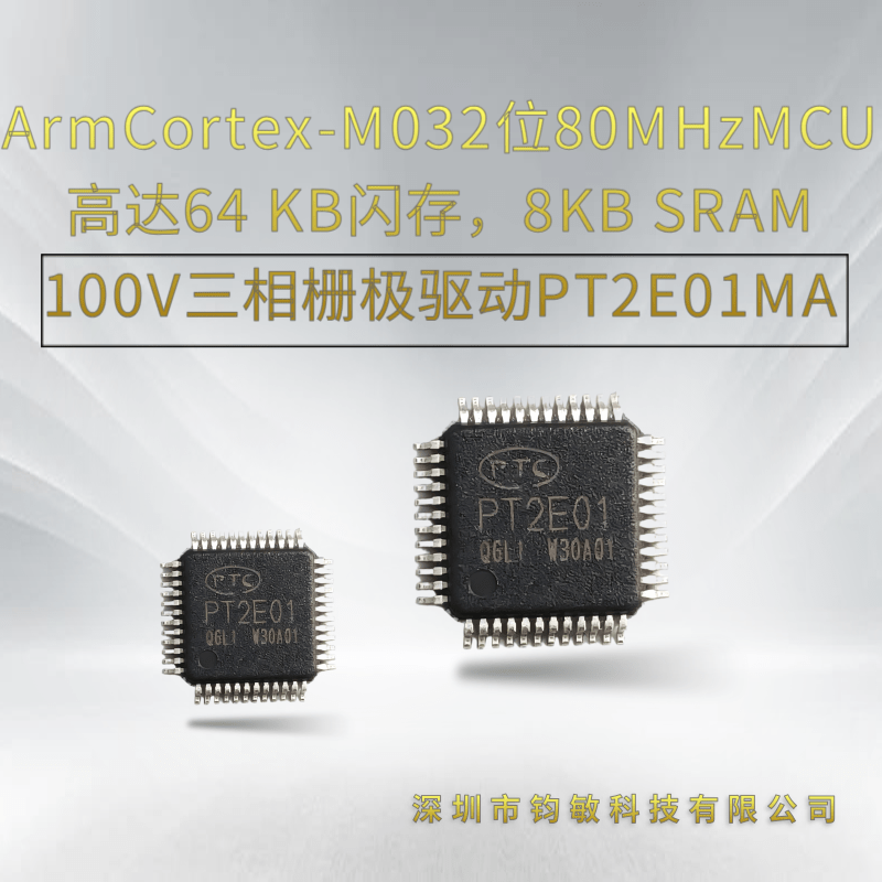
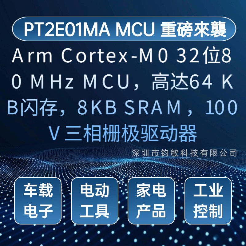


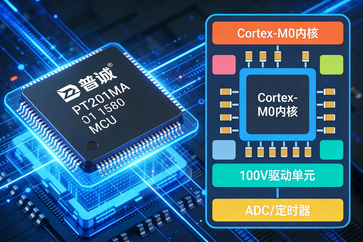
 | PT2E01MA Overview |
PT2E01MA System Block Diagram: | PT2E01MA Applications |
- **Core**
– ARM® 32-bit Cortex®-M0 MCU
– Maximum frequency: 80MHz
– System performance: 0.846 DMIPS/MHz (Dhrystone 2.1, zero-wait state)
- **Memory Units**
– 64K bytes Flash
– 8K bytes SRAM
- **Power and Reset Management**
– Digital and I/O power: VDDH = 2.0 ~ 5.5V
– Analog power: VDDA = 2.4 ~ 5.5V
– Three-phase gate power: VDRV_PWR = 10 ~ 20V
– Power reset: POR/PDR/BOR, Low-Voltage Detection (LVD)
– Low-power modes: SLEEP, STOP0, STOP1, STANDBY, and SHUTDOWN
- **Clock Source Management**
– External 4 ~ 32MHz crystal oscillator
– Internal 16MHz RC oscillator
– Internal 32KHz RC oscillator
– PLL (Phase-Locked Loop) circuit, maximum frequency multiplication up to 80MHz, supporting fractional frequency setting
- **I/O Resources**
– Up to 43 general-purpose I/Os
– Supports external interrupt events
– 8 I/Os supporting low-power external wake-up events
- **Timers**
– 1x 16-bit Enhanced Timer: 4 input captures / 6 output compares, 4 sets of complementary PWM outputs, supports brake function
– 2x 32-bit Advanced Timers: 2 input captures / output compares, 2 sets of PWM outputs (1 set of complementary PWM outputs)
– 2x 16-bit Advanced Timers: 4 input captures / output compares, 4 sets of PWM outputs (3 sets of complementary PWM outputs)
– 1x 16-bit Basic Timer
- **Communication Interfaces**
– 1x I2C: Multi-master mode, SMBus
– 2x SPI
– 2x UART: Supports automatic baud rate detection, RS-485, and hardware automatic flow control
- **Arithmetic Acceleration Unit**
– 1x CALC: 32-bit division and square root operations
- **Direct Memory Access (DMA) Controller**
– 6 DMA transfer channels
– Each channel has an independent control buffer to improve transfer rate
– Supports peripheral transfer requirements, including SPI, I2C, UART, timers, and ADC
– Supports data transfer between peripheral and memory (P2M/M2P) or between memory and memory (M2M)
- **Analog Control Unit**
– 1x 12-bit ADC: 2MSPS, 15 channels total, up to 11 external inputs
– 1x Analog Comparator (CMP)
– 1x Operational Amplifier (OPAMP): Configurable differential/single-ended PGA, supporting x1 ~ x32 gain
– 1x VRES: 5-bit resistor divider
- **System Peripherals**
– SWD (Serial Wire Debug) protocol debug interface
– System timer
- **Functional Safety and Information Security Modules**
– 128-bit UID (Unique Identification Number)
– Watchdog Timers: IWDT (Independent Watchdog Timer) and WWDT (Window Watchdog Timer)
– External crystal clock security detection (CSS)
– 8/16/32-bit CRC (Cyclic Redundancy Check) code with configurable generator polynomial
- **Other Additional Functions**
– 1x 100V-voltage-tolerant Three-Phase Gate Driver: Integrates 100V-voltage-tolerant half-bridge high-side drivers, capable of driving up to 3-phase half-bridge gates, with built-in dead-time control and shoot-through current protection
- **Package Type**
– LQFP48 (7x7mm)